By Ronald A. Miller, MS
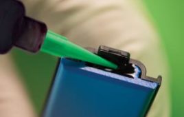
 Underfill applications use adhesive compounds to fill the gap between a microchip package and the printed circuit board (PCB). This is necessary because new types of chip packages, such as ball grid array (BGA) and chip-scale packages (CSP), are surface-mounted — meaning solder balls attach the bottom surface of the package to the PCB and provide the electrical connection.
This is different than the once-used dual-inline packages (DIP), which have metal leads that were inserted into holes in the PCB and soldered. These metal leads provided a secure mount to the PCB. However, the surface mount was prone to breakage of the solder connections to the PCB because of the thermal and mechanical stresses.
The epoxy adhesive is applied to one or more edges of the chip package and, when heat is applied, the adhesive flows by capillary action under the chip.
There are three methods of application:
- Full underfill: Covers the entire space between the chip package and the PCB
- Edge bonding: Fills only a short distance under the edge of the chip package
- Corner staking: Applies the adhesive at each of the four corners only
The important flow properties for the adhesive are:
- Low viscosity so the adhesive can flow into spaces as small as 0.1 mm
- Low thixotropy, which means that the viscosity of the adhesive remains constant over time when it is subject to a shear stress
- Good wetting to form a good bond to the chip package and the PCB
- Anti-foam properties to avoid air bubbles in the cured adhesive
The mechanical properties needed by the adhesive are toughness to resist drop impact, low thermal expansion coefficient to resist shear stresses, and low moisture absorption and penetration by chemicals to protect the solder connections from corrosion.


Tell Us What You Think!